Anatomy of a GPU1
To make it easier to understand the operation and structure of modern graphic units, we will look at a simplified description of the idea that led to their creation. In contrast to complex CPUs, GPUs aim to execute program code, which has a large number of relatively simple and repetitive operations, on a large number of small processing units. Among many problems that execute considerably faster on the modern GPUs are image and video processing, operations on large vectors and matrices, deep learning.
Modern CPUs are complex digital circuits that speculatively execute instructions in multiple pipelines. These instructions support many diverse operations and addressing modes. CPUs have built-in branch prediction units and trace caches, which store microcodes to be executed. Modern CPUs have multiple cores, each with several levels of cache memory. Hence, the modern CPUs occupy a lot of space on the chip and consume substantial amounts of energy. CPU cores are designed to minimize latency for one or two threads simultaneously.
In parallel computing, we strive to have as many simple, small and energy-efficient processing units as possible. These smaller processing units typically run at a clock speed several times lower than the CPU clock. Therefore, smaller processing units require a lower supply voltage and thus significantly reduce energy consumption. GPU cores are designed to handle a large number of concurrent, lightweight threads to maximize throughput.

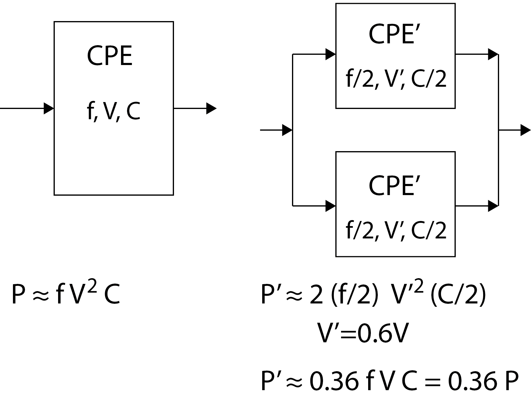
The figure above shows how we can reduce power consumption in a parallel system. On the left side of the image is a CPU solving a problem with frequency f. It needs energy obtained from the supply voltage V. The internal capacitance C acts as a kind of inertia resisting rapid changes in voltage levels of internal digital signals. The power required by the CPU for its operation is proportional to the clock frequency f, the square of the supply voltage V and the capacitance C.
The same problem is solved on the right side of the image but with two CPUs connected in parallel. Suppose we can break down our problem into two subproblems that we can solve separately, each on its CPU. Assume that new CPUs are half the CPU on the left side in terms of chip size and operate at a frequency of f/2. They also need less energy because they process instructions and data at half frequency. It turns out that when we halve the clock frequency in a digital system, we only need 60% of the supply voltage to operate the system. As each new CPU occupies half of the size of the lefthand side CPU, their capacitance is only C/2. Therefore, the new power P' required by a parallel system s only 0.36 P.
Evolution of a GPU
Suppose we want to add two vectors, vecA andvecB, using the C function vectorAdd () and save the result in the vector vecC:
1 2 3 4 5 6 7 | |
All vectors are 128 in length. We have intentionally used the while loop in the code to add all the corresponding elements of two vectors. The index of the current vector element was intentionally labelled as tid, which is an abbreviation of thread index. We will learn later why we chose such a name.
Vector addition on a CPU
To understand how to program massively parallel graphic processors, we must first understand how they are built. The basic principle of GPUs is to have many (hundreds or even thousands) simpler processing units simultaneously executing the same instructions on different data instead of one or two powerful CPUs. To understand how to build such an efficient massively parallel processor, we will first briefly describe how general-purpose CPUs are built.
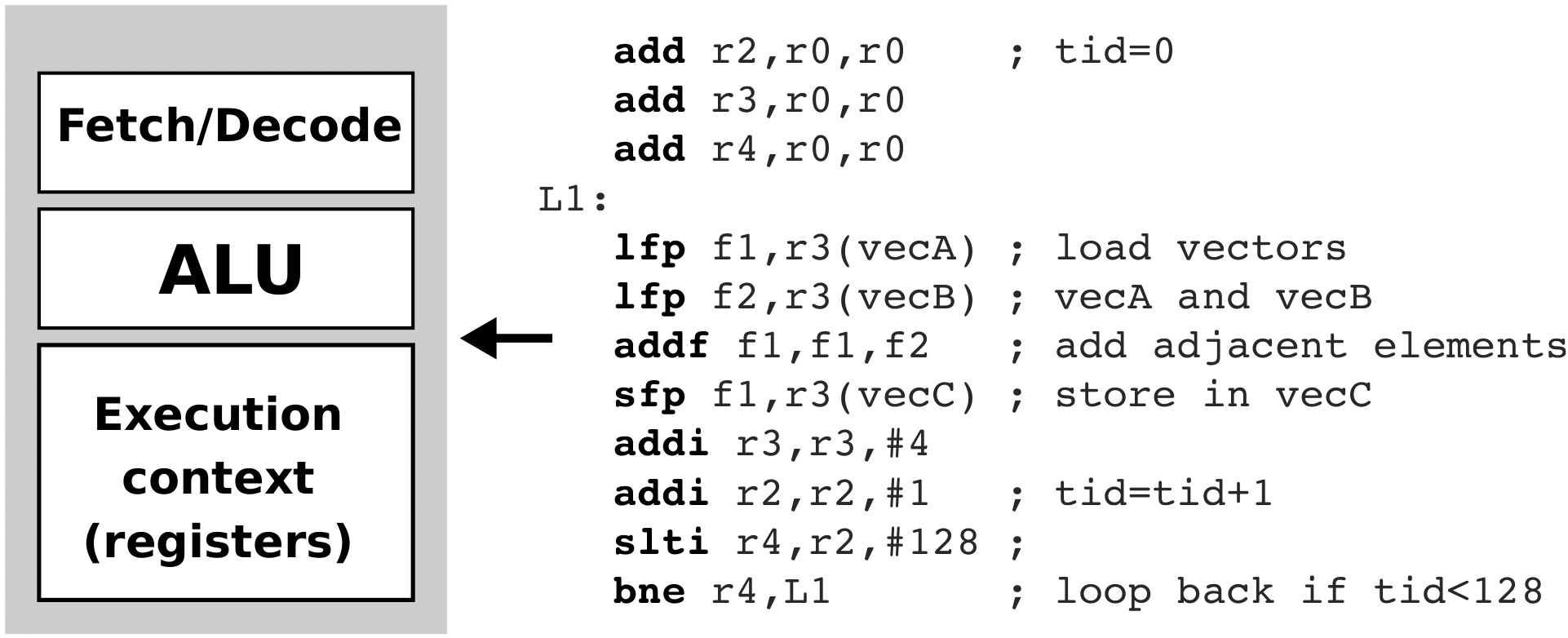
A CPU consists of the instruction fetch and instruction decode logic, an arithmetic-logic unit (ALU), and the execution context. The fetch/decode logic is responsible for fetching the instructions from memory, decoding them, preparing operands and selecting the required operation in ALU. The execution context comprises the state of the CPU, such as a program counter, a stack pointer, a program-status register, and general-purpose registers. Such a general-purpose single-core CPU with a single ALU and execution context can run a single instruction from an instruction stream (thread) simultaneously. For example, such a simple single-core CPU is presented in the figure below. Suppose you want to run the vectorAdd () function on such a simple CPU.

A compiled fragment of the function vectorAdd() that runs on a simple single-core CPU is presented on the righthand side in the above figure. With the first two instructions, we clear the registers r2 and r3 (suppose r0 is always zero). The register r2 stores the loop counter (tid), while the register r3 contains offset in the vectors VecA and VecB. Within the L1 loop, the CPU loads corresponding elements from the VecA and VecB into the floating-point registers f1 and f2, adds them and stores the result from the register f1 into the vector VecC. After that, we increment the offset in the register r3. Recall that the vectors contain 32-bit floating-point numbers; thus, the offset is incremented by 4. At the end of the loop, we increment the loop counter (variable tid) in the register r2 and compare the loop counter with the value of 128 (the number of elements in each vector). If the loop counter equals 128, we terminate the loop.
Vector addition on a two-core CPU
Instead of using one simple CPU core, we can use two such cores. Why? Using two CPU cores, we can execute two instruction streams fully in parallel (see figure below). A two-core CPU replicates processing resources (Fetch/Decode logic, ALU, and execution context) and organizes them into two independent cores. When an application features two instruction streams (i.e., two threads), a two-core CPU provides increased throughput by executing these instruction streams simultaneously on each core. We can now split the vector addition to run as two threads on each core. In this case, each thread will add 64 adjacent vector elements. Notice that both threads execute the same instruction stream simultaneously but on different data. The first thread adds the first 64 elements (the loop index tid in the register r2 iterates from 0 to 63), while the second thread adds the last 64 elements (the loop index tid in the register r2 iterates from 64 to 127).

Streaming multiprocessor and streaming processors
We can achieve even higher performance by further replicating ALUs and execution contexts, as in the figure below. Instead of replicating the complete CPU core, we can replicate only ALU and execution context, leaving the fetch/decode logic shared among ALUs. As the fetch/decode logic is shared, all ALUs should execute the same operation, but they can use different input data.

The figure above depicts a core with eight ALUs, eight execution contexts and shared fetch/decode logic. In addition, such a core usually implements additional storage for data shared among the threads.
Using only one instruction, we can add eight adjacent vector elements in parallel on such a core. The instructions are now shared across threads with identical program counters (PC) and executed simultaneously - i.e., every single instruction is performed in lockstep on different data. Thus, there is one ALU and one execution context per thread. Each thread should now use its ID (tid) to identify data to be used in instructions.
The pseudo assembly code executed on such a core is also presented in the above figure. When the first instruction is fetched, it is dispatched to all eight ALUs within the processor core. Recall that each ALU has its own set of registers (execution context), so each ALU would add its own tid to its register r2. The same also holds for the second and all following instructions in the instruction stream. For example, the instruction lfp f1,r3(vecA) is executed on all ALUs at the same time. This instruction loads the element from vector vecA at the address vecA+r3. Because the value in r3 is based on thread index (tid), each ALU will operate on a different element from vector vecA. Most modern GPUs use this approach where the cores execute scalar instructions. Still, one instruction stream is shared across many threads.
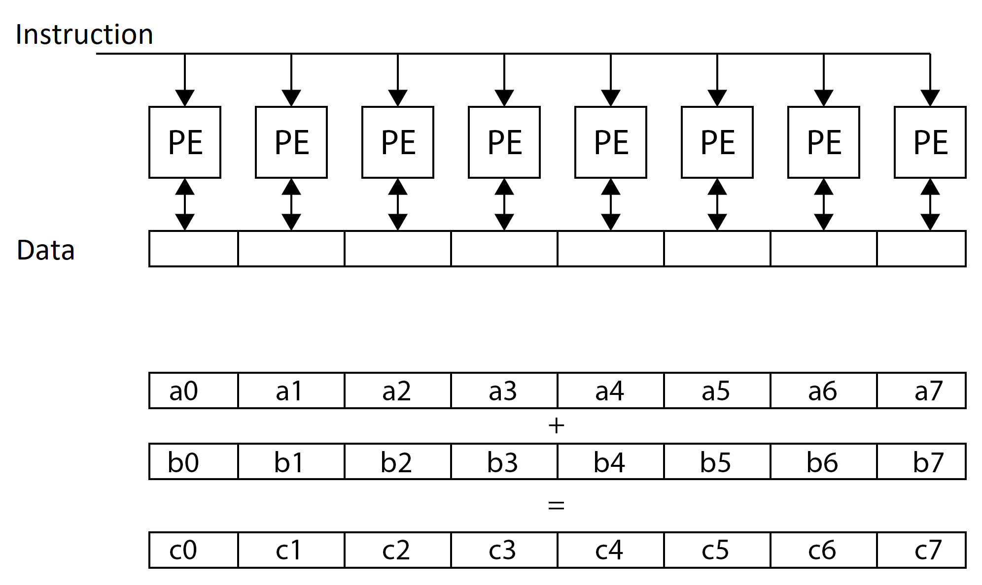
However, we can notice that such a CPU still has only one fetch/decode shared among eight ALUs - this means that it can only fetch, decode and execute only one instruction in one clock cycle! Therefore, such a CPU issues the same instruction to all arithmetic-logic units simultaneously and executes the instructions in a lock-step fashion. This time the operands in the instruction are vectors of length 8, which allows us to add eight consecutive elements of the vectors in one cycle (simultaneously) and repeat the loop only 16 times. We refer to such a processing unit as a streaming multiprocessor (SM) . A streaming multiprocessor can execute a single operation over a large amount of data simultaneously. This execution method is called SIMD (Single Instruction Multiple Data). As an SM executes each instruction in eight arithmetic-logic units simultaneously, it looks as if different threads are executed. Therefore, such implementation is also referred to as SIMT (Single Instruction Multiple Threads). Arithmetic-logic units that execute the same instruction over different operands are called streaming processors (SP). The figure below shows the SIMD (SIMT) execution of commands.

Each SP has its private set of registers. Therefore, an SM has also a tiny shared or local memory, used by threads to share data.
Graphics processing unit
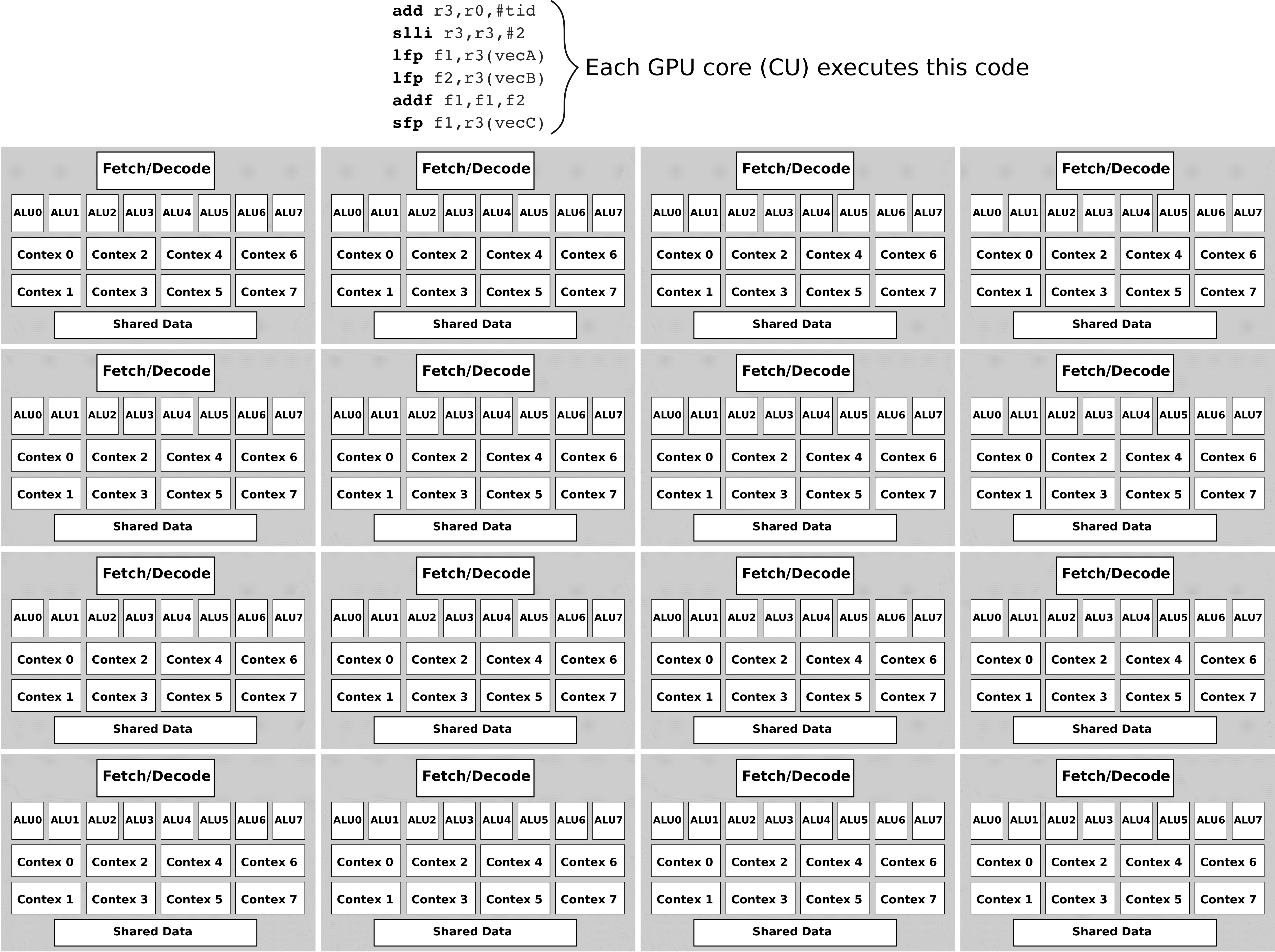
We can further improve the execution speed of our vector addition problem by replicating SMs - this is how GPUs are built. The figure below shows a GPU containing 16 SMs. Using 16 SMs, we can add 128 adjacent vector elements in parallel using one instruction stream. Each SM executes a code snippet (presented at the top of the figure). This code snippet represents one thread. Let us suppose that we run 128 threads, and each thread has its own ID, tid, where tid is in range 0 . . . 127. The first two instructions load the thread ID tid into r3 and multiply it by 4 (in order to obtain the correct offset in the floating-point vector). Now, the register r3 (recall that registers are private for each thread) contains the offset of the vector element that will be accessed in that particular thread. Each thread then adds two adjacent elements of vecA and vecB and stores the result into the corresponding element of vecC. Because each SM contains eight SPs (128 SPs in total), there is no need for the loop.
Hopefully, you can now understand the basic idea used to build GPUs: we use as many ALUs (SPs) as possible and let SPs execute same instructions on a lock-step basis, i.e., running the same instruction simultaneously but on different data.

Summary
The GPUs are built around an array of Streaming Multiprocessors (SM). GPU hardware parallelism is achieved through the replication of this architectural building block. Each SM in a GPU is designed to support the concurrent execution of hundreds of threads through the replication of Streaming Processors (SP), and there are generally multiple SMs per GPU, so it is possible to have thousands of threads executing concurrently on a single GPU.
All SMs in a GPU execute the same program (referred to as kernel), and all SPs within one SM execute the same instruction simultaneously. In this way, different SMs may execute different parts of the kernel. We also say that SMs execute groups of threads, and SPs execute individual threads.
-
© Patricio Bulić, University of Ljubljana, Faculty of Computer and Information Science. The material is published under license CC BY-NC-SA 4.0. ↩