Main phases
A high-level synthesis tool transforms the code in a higher-level language, such as C/C++, to the hardware of FPGA. It takes functions and automatically maps them onto the FPGA resources (wires, LUTs, registers, DSPs, block/ultra RAMs). This procedure undergoes three main phases:
- Scheduling
- Binding
- Control logic extraction
For an illustrative example, let's assume our input to HLS is a C code that implements the following function:
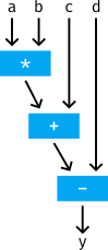
int f(char a, char b, char c, char d) {
    int y;
    y = a * b + c - d;
    return y;
}
The function f computes its output y using arithmetic operations (multiplication, addition, and subtraction) on the input bytes a, b, c, and d. First, we can convert the upper code to an intermediate representation using a graph that resembles data dependencies between operations.
Scheduling Phase
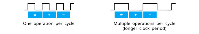
Our high-level code is untimed: it only says what to do and not when to do it. However, to implement this behaviour in FPGA, we must specify the timing for every operation. This is a job for the scheduling phase that assigns a time slot to each operation, i.e. in exactly which clock cycle this operation will take place.
The scheduler considers the device's clock cycle length and the required time for certain operations to complete. Some operations need to be spanned over multiple clock cycles. On the other hand, if the clock period is longer or the target FPGA is faster, HLS can schedule more operations in a single clock cycle.
Binding Phase
Binding is the process of mapping operations to specific hardware resources such as logic and memory blocks. It involves selecting the hardware components to implement each operation in the scheduled timeline.
Following our example, let's take a closer look at a binding phase consisting of the initial and target steps.
The scheduling phase places the multiplication of a and b and subsequent addition of c in the first clock cycle. The final result y is available in the second clock cycle after the subtraction of d. An internal register is used to pass results between clock cycles, which stores the data on the rising edge of a clock.
- The initial step of a binding phase implements the multiplication using a combinational multiplier (mul). In digital logic, addition and subtraction are, in fact, the same operation - subtraction is the addition of the opposite: a - b = a + (-b). Here, we use a combinational adder/subtracter (add sub) for these operations.
- In the target step, binding further optimizes the resource allocation. The multiplication and addition are now implemented using a special operation called multiply-accumulate (MAC), performed on the DSP block, a part of the FPGA chip (see info box for details). In this way, a better balance between throughput and power efficiency is achieved.
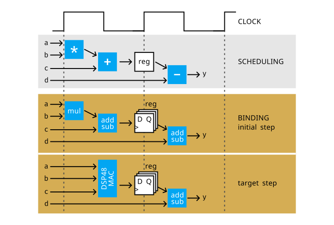
DSP48 block
The AMD/Xilinx DSP48 component is a low-power building block of an FPGA device intended for digital signal processing applications. It integrates an 18-bit by 25-bit signed multiplier with a 48-bit adder. This combination of multiplication and addition within a single block enables the execution of complex mathematical operations in a highly streamlined manner. Specifically, the operation multiply-accumulate (MAC) is relevant here, as the block facilitates the simultaneous multiplication and accumulation of values, contributing to improved computational efficiency in tasks like dot product and matrix multiplication.
Control Logic Extraction
In the previous straightforward example, a function invocation entailed a single input data pass through the logic over two clock cycles, eliminating the necessity for logic governing data flow control. Let's consider another example to delve deeper into how HLS handles loops. Building upon the earlier code, we introduce arrays and a loop. The function f executes the same processing as before but now operates on three elements within an array encapsulated in a for-loop structure.
void f(int in[3], char b, char c, char d, int out[3]) {
    int a, y;

    for(int i = 0; i < 3; i++) {
        a = in[i];
        y = a * b + c - d;
        out[i] = y;
    }
}
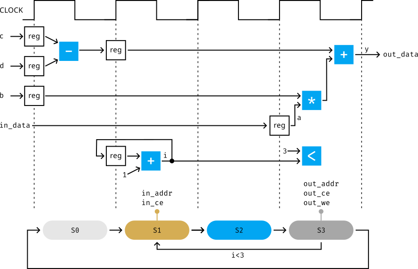
In this phase, HLS transforms the top-level function arguments into input/output ports within an RTL module, a process called I/O port implementation. These ports serve as the interface for the module. In our specific example, scalar values of type char are realized as an 8-bit bus. Typically, arrays are mapped onto BRAM, although alternative options like LUTs or registers exist. To access a BRAM component, HLS generates data (_data) and address ports (_addr), along with control signals for chip-enable (_ce) and write-enable (_we).
To facilitate the execution of a loop over diverse data using a shared logic structure, HLS automatically generates a control unit as a finite state machine (FSM). This process, known as control logic extraction, oversees the data storage in internal registers and controls I/O signals. The FSM operates with a finite set of states, and state transitions occur exclusively on clock edges, constituting a synchronous process.
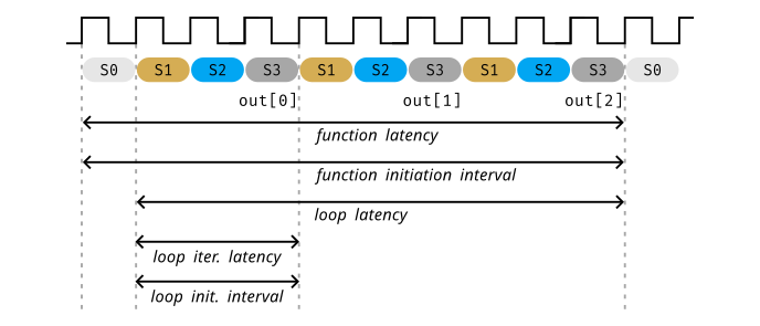
For the loop control in our example, HLS extracts an FSM with four states:
S0: The initial state, where a computation using an adder/subtracter yieldsc - d, a constant value throughout loop iterations.S1: The first stage of the loop, responsible for generating the address (in_addr) and chip-enable signal (in_ce) to retrieve an element from theinarray. Additionally, an adder counts the number of loop iterations. Upon reaching three iterations, the design returns fromS3toS0and recommences the process with new values ofcandd.S2: The BRAM returns the data element on thein_databus, buffering its value in the registera.S3: Computation ofyoccurs using the value on the input portb, the precomputed value ofc - dfromS0, and the dataastored in the register. The control unit generates signals for enabling and addressing BRAM (out_addr,out_ce,out_we), storingyas an element in theoutarray.
The FSM cyclically transitions through states {S1, S2, S3} three times before reverting to the initial state S0, initiating the entire process anew with updated values of input arguments.
Using the previous example, let's define and illustrate the following performance metrics:
- function latency (10 cycles): the number of clock cycles necessary for the function to transition from processing input to generating output. When the output forms an array, the latency is measured up to the point of generating the last value within the array.
- function initiation interval (10 cycles): the number of cycles before the function can initiate a new set of input reads and start to process the next set of input data.
- loop latency (9 cycles): the number of cycles to execute all loop iterations.
- loop iteration latency (3 cycles): the number of cycles it takes to complete one loop iteration.
- loop initiation interval (3 cycles): the number of clock cycles before the next loop iteration starts to process data.
In the upcoming section, we introduce Xilinx Runtime (XRT), an open-source software stack streamlining FPGA utilization for compute-intensive tasks, with a focus on AMD Alveo U250 boards.