FPGA Basics
Field-programmable gate array (FPGA) represents a unique and flexible approach within the realm of application-specific integrated circuits (ASIC). While ASIC chips are custom-designed digital devices optimized for specific tasks, FPGAs provide a reconfigurable platform that bridges the gap between general-purpose processors and dedicated hardware.
Unlike "traditional" ASICs (see ASIC vs. FPGA dilemma box for explanation), FPGAs allow users to define and modify their logical functionality after manufacturing, offering adaptability similar to software-based systems. This programmability is achieved through a sea of configurable logic blocks (CLB) and interconnects, enabling the implementation of various digital circuits. FPGAs find extensive use in rapid prototyping, hardware acceleration, and applications where the ability to reconfigure hardware dynamically is advantageous.
Despite its inherent flexibility, an FPGA device may exhibit lower performance and power efficiency than a non-programmable ASIC for specific specialized tasks, choosing between the two depending on the particular requirements of the application at hand.
ASIC vs. FPGA dilemma
What is the relationship between ASIC and FPGA circuits? Are they from different planets or the same family? Well, an application-specific integrated circuit is a semiconductor chip tailored for a specific application, offering optimized performance and power efficiency.
We can classify ASIC into three main categories:
These ASICs are designed from scratch, allowing for complete customization of the chip's layout and functionality. Full custom ASICs provide the highest level of performance but often involve higher development costs and longer design cycles.
Semi-custom ASICs involve a mix of custom and predefined components. They can be further classified into:
- Cell-Based Integrated Circuit (CBIC): Utilizes predefined standard cells, including logic gates, flip-flops, and other essential components. It provides a balance between customization and design efficiency.
- Gate Array (GA): Features predefined logic gates and a flexible interconnect structure, allowing limited customization. GA offers a faster design turnaround compared to full custom ASIC.
These ASICs provide flexibility through programmability and can be further divided into:
- Programmable Logic Devices (PLD): Includes devices like PALs (Programmable Array Logic) and GALs (Generic Array Logic) with fixed architectures that can be programmed to perform specific functions.
- Complex Programmable Logic Devices (CPLD): More complex than PLDs, offering a higher level of programmability and functionality.
- Field-Programmable Gate Arrays (FPGA): we are here now. So, FPGA is just a subcategory in the ASIC world – a family member.
Key Theoretical Principles
With digital systems like FPGA, we want to implement a device to process and manipulate digital signals. To achieve this, we use building blocks in the form of Boolean functions that describe combinational (output is based on the inputs only) or sequential (output depends on the input history as well) logic. To explain this, let's take a look at the following example.
Let's have three inputs x1, x2, and x3. We can imagine they are wall switches. We also have a light bulb, let's call it y. It is a special bulb that glows only when this sophisticated condition is met:
- x1 is "off" and x2 is "on" and x3 is "on" or
- x1 is "on" and x2 is "off".
We can describe such a condition using the Boolean function f:
y = f(x1, x2, x3) = x̅1x2x3 ∨ x1x̅2 .
Now, we can implement the function f using wires and logic gates such as NOT, AND, and OR, as illustrated in the left part of the figure below. Another method to represent a function is through a truth table. For every conceivable combination of inputs, we assign the corresponding output value. This approach serves as a foundational step in comprehending the implementation of Boolean functions in an FPGA. Following our example, let's document the truth table on the right side of the diagram.
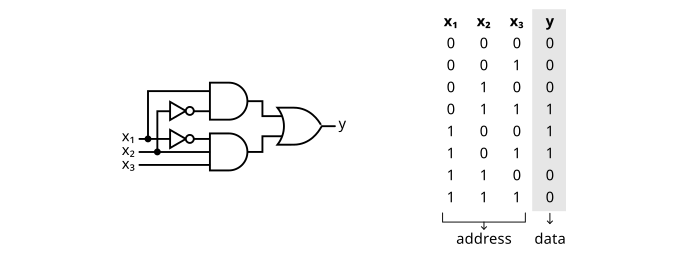
We can also see the truth table as a memory, where inputs define the address that points to a stored data piece. In our case, we have a memory that can hold 8 bits. In the FPGA world, such a memory is called a lookup table (LUT) – it provides the mapping between inputs and output. When LUT has three inputs, it is called LUT3.
Did you know
In 1985, company Xilinx introduced the initial commercially feasible FPGA, known as the XC2064. It was equipped with 64 configurable logic blocks, each containing two three-input lookup tables, i.e. LUT3.
LUTs are a great way to implement logic functions in FPGA. Suppose we do not have any LUT3 in our target FPGA chip now, only an abundance of LUT2. Can we still implement the desired function f? Yes, with a little help from a friend called function decomposition.
We decompose the truth table of a function into upper and lower parts based on the input x1. We get two smaller truth tables: the first (upper) is valid when x1=0, while the other is when x1=1.
Thus, we get two two-input LUTs (LUT2) that are being addressed by x2 and x3. To get the output y, we must select between the two LUTs considering the value of x1. We achieve this with a logic element called multiplexer (MUX).
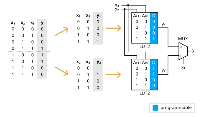
We have just learned that we can implement any three-input function using only LUT2 elements. With the principle of function decomposition, virtually any n-input function can be realized using LUTs with fewer inputs than n. A LUT is usually implemented by small static RAM, and its content is initialized by programming an FPGA chip.
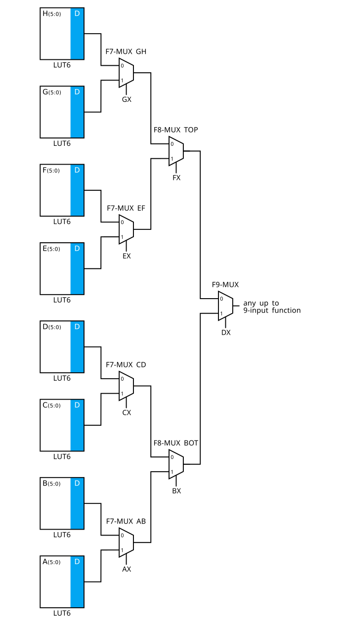
9-input function using LUT6 (click to learn more)
The diagram describes a modern Xilinx FPGA based on UltraScale architecture focusing on the hierarchy of MUXs and LUTs that can implement any up to 9-input function.
Architecture
The primary building block of an FPGA chip is a slice, which can implement Boolean functions through the use of lookup tables (LUT), multiplexers (MUX), and storage elements known as flip-flops (FF). Typically, a slice also features dedicated carry logic for performing arithmetic addition and subtraction. The figure below illustrates a slice segment containing a LUT6 function generator, an F7-MUX enabling the construction of broader functions, two configurable MUXs for internal signal routing, and two D-type FFs. Each slice typically incorporates eight such segments in modern FPGA architectures, such as Xilinx UltraScale. LUTs in some slices can be configured as distributed RAM or shift registers.
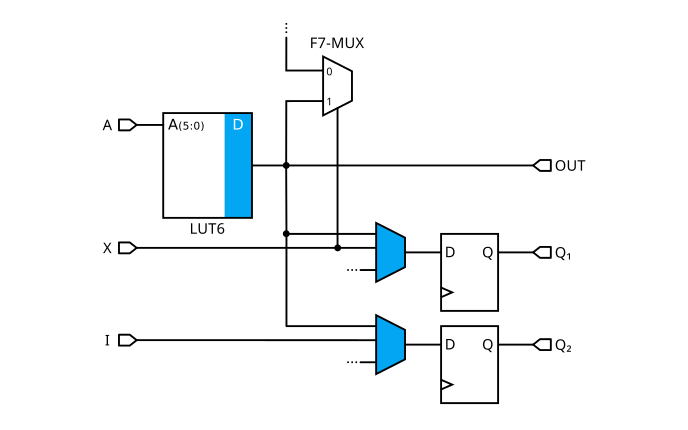
Please note that the programmable elements in the figures are highlighted in blue ■.
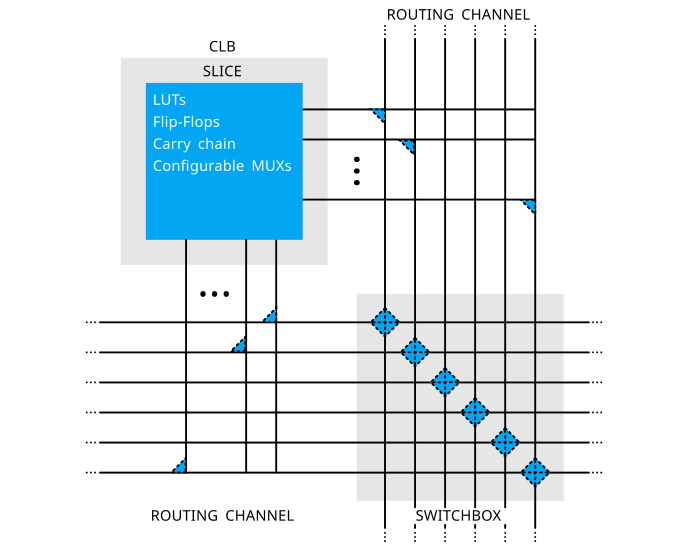
Moreover, one or more slices are enclosed in a Configurable Logic Block (CLB) that is connected to other CLBs through a programmable network of interconnections. In the diagram below, you can see wires that run over horizontal and vertical routing channels. The switchbox contains multiple switches that permit flexible wiring configurations between the different routing tracks in the routing channels adjacent to the switchbox.
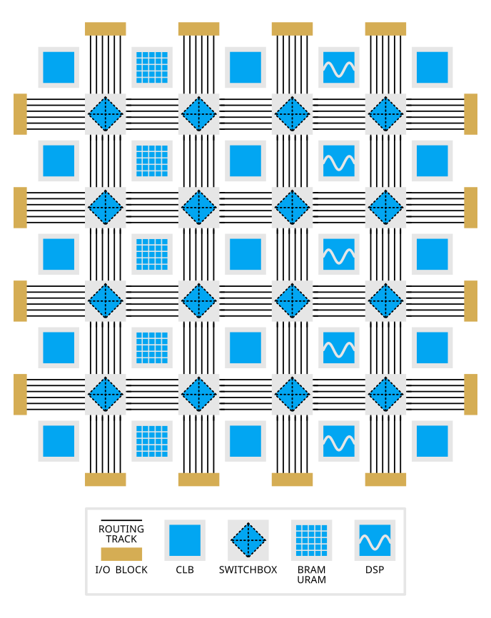
In addition to CLBs and the programmable routing mechanism, FPGA chips typically consist of three additional types of building blocks:
-
Input-output blocks (I/O blocks) that facilitate the connection of the FPGA to external input and output devices.
-
Dedicated memory blocks such as Block RAM (BRAM) and UltraRAM (URAM) that provide on-chip memory resources. URAM extends the memory capacity of BRAM to meet the demands of more substantial and data-intensive tasks in modern FPGA designs.
-
Digital Signal Processing (DSP) blocks are designed to perform mathematical operations such as multiplication and accumulation efficiently, which are fundamental in digital signal processing.
Hardware under the hood (click to learn more)
HPC clusters participating in the EuroHPC initiative allocate specific compute nodes to FPGA accelerators. Notably, clusters such as Complementary Systems and NSC incorporate nodes equipped with AMD Alveo U250 and U280 accelerator cards.
Here is a snippet from the AMD Alveo U250 data sheet to provide an overview of the rich abundance of FPGA resources:
- FPGA chip: UltraScale+ XCU250-2LFIGD2104E
- LUTs: 1,727,040
- FFs: 3,454,080
- DSP slices: 12,288
- Block RAMs: 2,688
- UltraRAMs: 1,280
- RAM: 64 GB DDR4, 77 GB/s
- PCIe interface Gen3 x16
- Two 100 Gbps network interfaces (2×QSFP28)
Today's FPGA architecture comprises thousands of the aforementioned blocks arranged in a grid structure, depicted in a simplified form in the following figure.
In the upcoming section, we explore the fundamentals of high-level synthesis (HLS), a focal point of this workshop. In utilizing HLS tools successfully, it's usually not essential to delve into every intricate detail of FPGA architecture. Instead, a more crucial aspect is understanding the diverse FPGA resources and how HLS optimizations impact resource utilization.