Memory Hierarchy1
In general, applications do not access arbitrary data or run arbitrary code at any point in time. Instead, applications often follow the principle of locality, which suggests that they access a relatively small and localized portion of their address space at any point in time. There are two different types of locality:
- Temporal locality (a locality in time) and
- Spatial locality (a locality in space).
Temporal locality assumes that if a data location is referenced, it is more likely to be referenced again within a short time. Spatial locality assumes that if a memory location is referenced, nearby locations are likely to be referenced. Modern computers use a memory hierarchy of progressively lower-latency but lower-capacity memories to optimize performance. This memory hierarchy is only useful because of the principle of locality. A memory hierarchy consists of multiple levels of memory with different latencies, bandwidths, and capacities. The CUDA memory model unifies separate host and device memory systems and exposes the full memory hierarchy so that you can explicitly control data placement for optimal performance. The CUDA memory model exposes many types of programmable memory to you:
- Registers,
- Shared memory,
- Constant memory,
- Texture memory, and
- Global memory.
Each level of the hierarchy has a different access time, presented in the table below (access time is measured in clock cycles):
| Memory | Access time |
|---|---|
| Registers | 1 |
| Shared memory | ~5 |
| Constant memory | ~500 |
| Texture memory | ~500 |
| Global memory | ~500 |
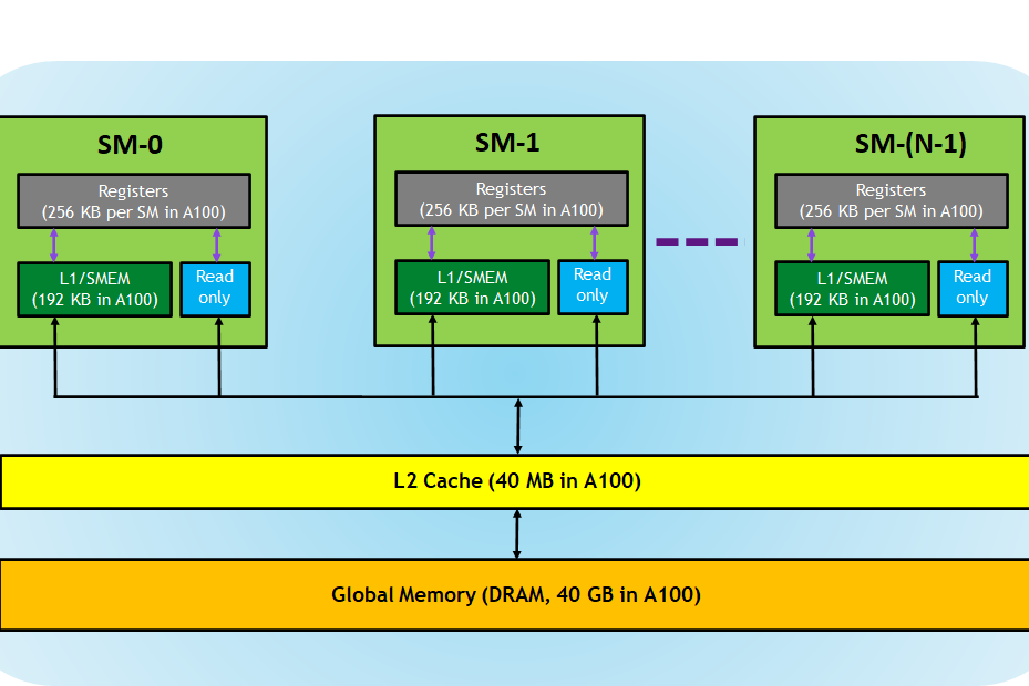
CUDA-capable GPUs have a memory hierarchy as depicted in the figure below:

Registers
Registers are a very important memory resource. Registers are the fastest memory space on a GPU. An automatic variable declared in a kernel without any other type qualifiers is generally stored in a register. Registers are private to each thread, meaning registers assigned to a thread are not visible to other threads. The compiler makes decisions about register utilization. Each SM has 64k 32-bit registers shared equally by the thread blocks concurrently executing on the SM. Recall that there is a limit of 64 concurrent warps (equivalent to 2k threads) that can execute on a given SM. This means that if the compiler allows a thread to use more than 32 registers, the maximum number of thread blocks running on the SM (i.e. occupancy) is reduced, potentially harming performance. Contrary, using fewer registers in your kernels may allow more thread blocks to reside on an SM. More concurrent thread blocks per SM can increase occupancy and improve performance.
For example, each SM in the Tesla K40 (Kepler microarchitecture) has 65,536 registers, and each thread can use a maximum of 255 registers. Suppose we have 120 thread blocks with 128 threads per block. On the Tesla K40 with 15 SMs, we will have eight thread blocks per SM (120/15 = 8), with each thread using up to 64 registers (65536 / (8 * 128) = 64).
L1/Shared memory
Each SM has a fast, on-chip scratchpad memory that can be used as L1 cache and shared memory. All threads in a thread block can share shared memory, and all thread blocks running on a given SM can share the physical memory resource provided by the SM. Because shared memory is on-chip, it has much higher bandwidth and much lower latency than global memory. Each SM has a limited amount of shared memory that is partitioned among thread blocks. Therefore, you must be careful to not over-utilize shared memory or you will inadvertently limit the number of active warps. Shared memory is declared in the scope of a kernel function but shares its lifetime with a thread block. When a thread block finishes execution, its shared memory allocation will be released and assigned to other thread blocks. The most critical aspect of shared memory is that it serves as a primary means for inter-thread communication. Threads within a block can cooperate by sharing data stored in shared memory.
For example, the Tesla K40 accelerator has 64kB of L1/Shared memory that can be configured in three different ways:
- 16 kB L1 and 48 kB shared memory
- 32 kB L1 and 32 kB shared memory
- 48 kB L1 and 16 kB shared memory.
Read-only memory
Each SM has an instruction cache, constant memory, texture memory and read-only cache, which is read-only to kernel code.
Constant memory resides in device memory and is cached in a dedicated, per-SM constant cache. Constant memory allows a single data to be sent to all threads at once (broadcasting). Texture memory resides in device memory and is cached in a per-SM, read-only cache. Texture memory is a type of global memory that is accessed through a dedicated read-only cache. Texture memory is optimized for a 2D spatial locality, so threads in a warp that use texture memory to access 2D data will achieve the best performance.
L2 cache
The L2 cache is shared across all SMs, so every thread in every CUDA block can access this memory. For example, the NVIDIA A100 GPU (Ampere microarchitecture) has an L2 cache size of 40 MB.
Global memory
This is analogous to the main memory of a CPU; the kernel itself and all data reside here. Global memory is the largest, highest-latency, and most commonly used memory on a GPU. The name global refers to its scope and lifetime. Data in global memory can be accessed on the device from any SM throughout the application's lifetime. The CPU can write and read data to and from the GPU's global memory. These exchanges go via the PCI bus and are relatively slow; therefore, we should design CUDA programs to minimize data transfers. In addition, data in the GPU global memory is preserved between kernel calls so that data can be reused by successive kernel calls without the need to reload. The global memory space is implemented in high-speed GDDR, which achieves very high bandwidth but has a high latency like all DRAM memories.
Reads and writes to global memory are always initiated from SM and are always 128-byte wide, starting at the address aligned at the 128-byte boundary. The memory blocks accessed in one memory transaction are called segments. This has an extremely important consequence. If two threads from the same warp access two data that fall into the same 128-byte segment, data is delivered in a single transaction. If, on the other hand, there is data in a segment that no thread requested—it is being read anyway, and you waste bandwidth. And if two threads from the same warp access two data that fall into two different 128-byte segments, two memory transactions are required. The important thing to remember is that to ensure memory coalescing, we want threads from the same warp to access contiguous elements in memory to minimize the number of required memory transactions.
Memory coalescing
Coalesced memory access or memory coalescing refers to combining multiple memory accesses into a single transaction. Grouping of threads into warps is not only relevant to computation but also to global memory accesses. The GPU device coalesces global memory loads and stores issued by threads in a warp into as few transactions as possible to minimize DRAM bandwidth. On the recent GPUs, every successive 128-byte memory block can be accessed by a warp in a single transaction.
A programmer's perspective
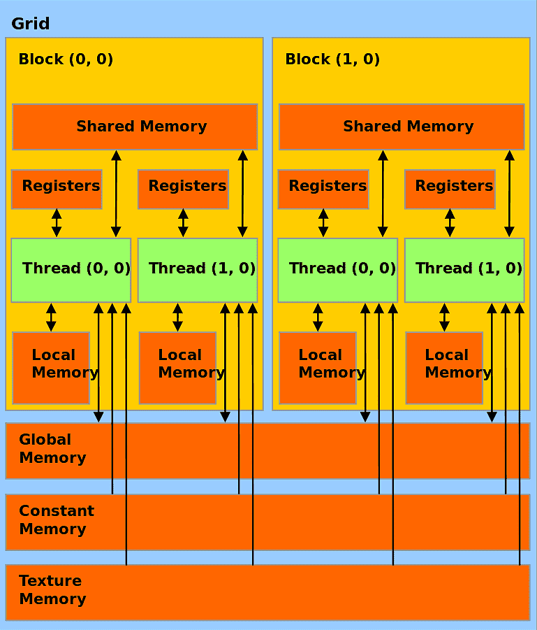
CUDA threads may access data from multiple memory spaces during their execution, as illustrated in the image below. Each kernel launches many threads - these threads from a kernel are referred to as a grid. Each thread has private registers. Each thread block has shared memory visible to all threads in the block and with the same lifetime as the block. All threads have access to the same global memory. There are also two additional read-only memory spaces accessible by all threads: the constant and texture memory spaces. The global, constant, and texture memory spaces are persistent across kernel launches by the same application.

-
© Patricio Bulić, University of Ljubljana, Faculty of Computer and Information Science. The material is published under license CC BY-NC-SA 4.0. ↩