Matrix-Vector multiplication
Let us now take a look at the matrix-vector multiplication. We will start with the simple version to illustrate the interfaces of the synthesized kernel. Next, we will cover the interfaces of the synthesized kernel. Then, we will analyze the performance of this simple version and extend it to the version that employs local memory.
Naïve implementation of matrix-vector multiplication
Unlike in the previous part, we will focus only on the kernel code. The host code, is almost indetical to one we saw in the example of vector addition. The host code, for example, can be found in the code repository.
The complete program for the naïve version of matrix-vector multiplication is given as:
1 2 3 4 5 6 7 8 9 10 11 12 13 14 15 16 17 18 19 20 | |
matv_mult implements matrix-vector multiplication for square matrices of dimension dims. The function takes three pointers to integer arrays as input: c (output vector), a (input matrix), and (input vector). The function utilizes two nested loops for matrix-vector multiplication, where the outer loop iterates over each row of the matrix a, and the inner loop performs the dot product of the corresponding row with the input vector b. The result is stored in the output vector c.
The #pragmaHLS directives specify the memory interface properties for high-level synthesis (HLS) targeting FPGA acceleration. Specifically, #pragma HLS interface m_axi is applied to the pointers a, b, and c, representing the input matrix, input vector, and output vector. These pragmas specify the use of the AXI memory-mapped protocol, facilitating high-bandwidth data transfer between the FPGA and global memory. A scalar interface pragma, #pragma HLS interface s_axilite, is employed for the variable dims, allowing it to be configured at runtime through an AXI Lite interface. This provides a lightweight control interface for adjusting the matrix dimension dynamically. These pragmas collectively guide the synthesis process, optimizing the hardware architecture for efficient memory access and configurability in the context of FPGA acceleration.
AXI protocol, AXI Memory mapped and AXI LITE interface
All the Xilinx blocks use AXI protocol to communicate with each other and their environment. The AXI (Advanced eXtensible Interface) is a widely used protocol in FPGA and ASIC designs, providing a standardized and high-performance interface for efficient communication between different hardware components. AXI defines rules and conventions for data transfer, addressing, and control signals, facilitating the integration of IP (Intellectual Property) cores and peripherals within a system-on-chip (SoC) or FPGA architecture. Its key features include support for burst transfers, multiple outstanding transactions, and configurable data widths, making it versatile and suitable for a broad range of applications in digital design.
Vitis HLS supports various AXI4 interfaces, including the AXI4-master (m_axi), AXI4-Lite (s_axilite), and AXI4-Stream (axis) interface. AXI4 memory-mapped (m_axi) interfaces in Vitis HLS facilitate efficient reading and writing of data in global memory, including DDR, HBM, and PLRAM. These interfaces serve as a convenient means of data sharing across different components of an accelerated application, enabling seamless communication between the host and kernel or among kernels on the accelerator card. The m_axi interface offers distinct advantages, including separate and independent read and write channels, support for burst-based accesses with a potential performance of approximately 17 GBps, and the ability to handle outstanding transactions.
In Vitis HLS, an HLS IP or kernel can be controlled by a host application or an embedded processor through the Slave AXI4-Lite interface (s_axilite), functioning as a system bus for communication between the processor and the kernel. This interface allows the host or embedded processor to initiate and halt the kernel and perform read or write operations on it. During synthesis in Vitis HLS, the s_axilite interface is implemented as an adapter, capturing communicated data from the host in registers on the adapter. The Vitis Kernel flow automatically infers the s_axilite interface pragma, providing offsets to pointer arguments assigned to m_axi interfaces, scalar values, and function return types.
Synthesized block
After everything is explained, we can visualize our synthesized kernel with the below image:
The main takeaways from the presented figure are as follows:
- The calculations performed within loops for matrix-vector multiplication are directly mapped to the compute logic during synthesis.
- The synthesized block establishes communication with global memory via AXI MM (Advanced eXtensible Interface Memory-Mapped) adapters.
- Ports
aandcshare AXI MM adapters as they belong to the same AXI bundle. This connection is defined using the bundle option. The rationale behind this bundling is rooted in the AXI protocol, which has separate channels for reading and writing, each with distinct addresses. - The value of the argument
dimsis acquired through the S_AXILITE adapter, facilitating lightweight control access for the specified variable.
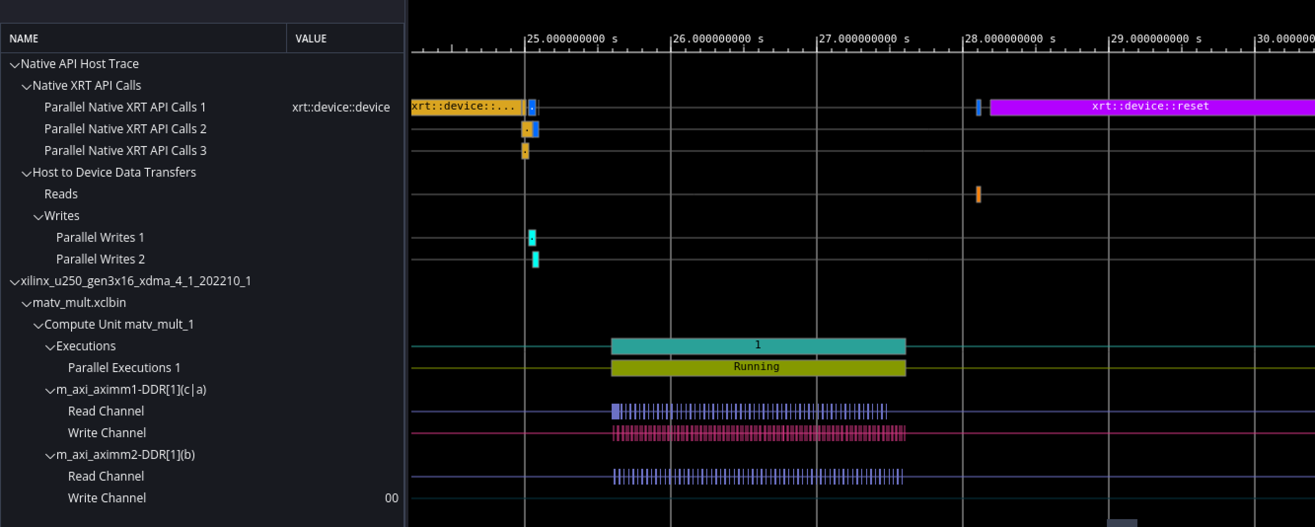
When we synthesize the our design for hardware emulation, we get the following signal traces in Vitis's analyzer:

Let's analyze the obtained traces. We have two groups of signals. One represents the signals corresponding to kernel loading, transferring the buffers, reading back the results, and stopping the accelerator. In the lower half of the diagram, we can notice the signals that correspond to the execution of kernels.
The representation of blue and green traces depicts the execution phases of the generated processing element. At the same time, the memory transfer dynamics reveal the presence of two separate memory interfaces, each associated with different AXI MM adapters. The choice of employing two banks aims to enable parallel reading of both the vector and matrix components. However, an inefficiency in memory access is observed, characterized by substantial delays incurred with each interaction with global memory, indicating a suboptimal access pattern that impacts overall system performance.
The above code is published in folder 02-matv_mult-naive of the workshop's repo.
Optimizing memory access
Optimizing data movement between the FPGA-accelerated kernel and external global memory is crucial for the performance of acceleration applications. Reading and writing data from external DDR SDRAM inherently incurs latency overhead. A strategically designed kernel seeks to minimize this latency impact, aiming to fully harness the available data bandwidth offered by the acceleration platform. This optimization is crucial for achieving efficient and high-performance execution of FPGA-accelerated applications.
One strategy for optimizing memory access is the implementation of a memory hierarchy. Unlike CPUs or GPUs, FPGAs lack a built-in hierarchical organization of memory. Nevertheless, this limitation doesn't limit us from creating our own hierarchy. The concept is straightforward: we establish local memory blocks to reduce the frequency of accesses to global memory or, at the very least, coalesce them. The following code illustrates this approach, aiming to enhance memory access efficiency for our kernel.
1 2 3 4 5 6 7 8 9 10 11 12 13 14 15 16 17 18 19 20 21 22 23 24 25 26 27 28 29 30 31 32 33 34 35 36 37 38 39 40 41 42 43 44 45 46 47 48 49 50 | |
Examining the code, a notable similarity with the previous kernel becomes evident. While this version may be less efficient for CPU execution than the previous one, its significance becomes apparent in FPGA implementation. The kernel's local arrays (a_local, b_local, and c_local) are synthesized as distributed RAMs, which the compute logic can access more rapidly than global memory. The data from global memory is first loaded into distributed RAMs corresponding to the local arrays a_local and b_local. Subsequently, the compute logic accesses matrix and vector elements from these distributed RAMs, facilitating the calculation of the matrix-vector product. The computed results are stored in a distributed RAM corresponding to the c_local array. Finally, the synthesized kernel then transfers data from the c_local array back to the global memory. This synthesized kernel, illustrated in the accompanying figure, leverages the local memory distributions for optimizing memory access in FPGA implementation.
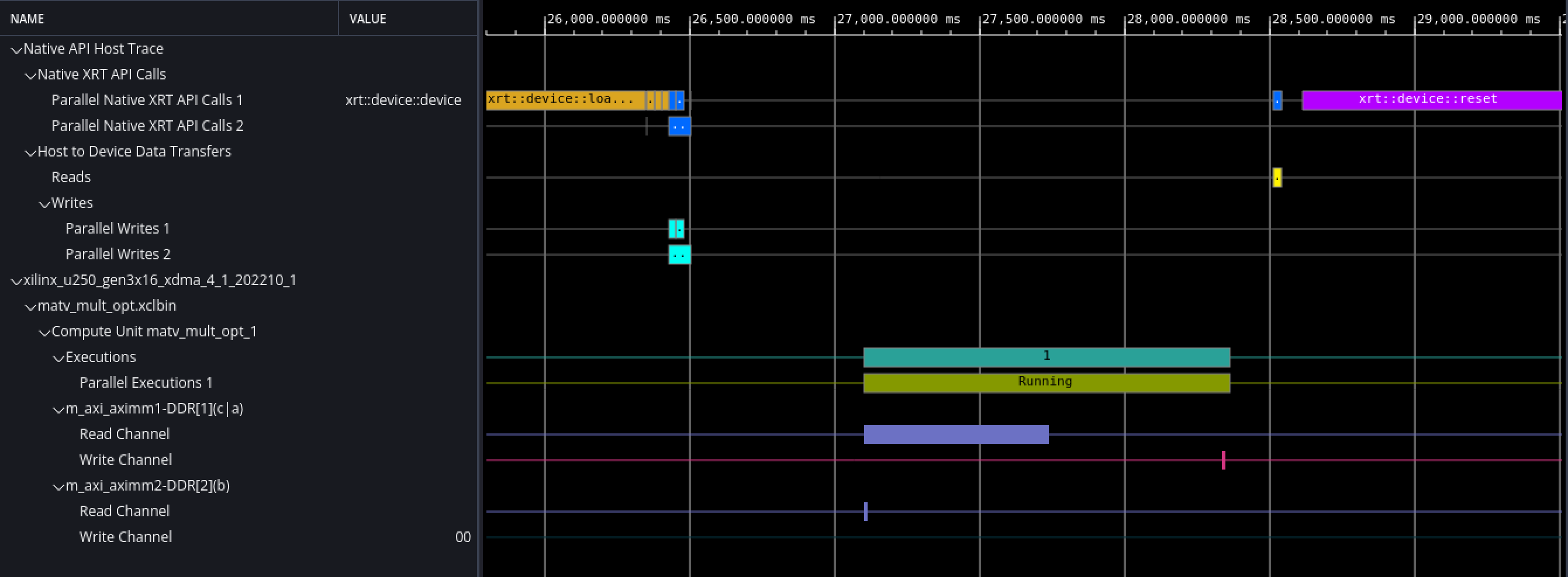
Furthermore, we adjust the options for the AXI MM interface, specifically enabling burst reads and writes. This enhancement further optimizes the data movements between the kernel and global memory. Following the emulation of the design at the hardware level, the resulting traces illustrate the cumulative impact of these optimizations on the overall performance.

In contrast to the previous traces, it is evident that the optimized kernel exhibits a reduced number of reads for the vector b and stores for the vector c. Notably, the memory access for elements of the matrix a has been effectively coalesced, leading to faster processing. These improvements highlight the efficiency gains achieved by strategically utilizing local memory blocks and fine-tuning AXI MM interface options.
The above code is published in folder 03-matv_mult-opt of the workshop's repo.